NIST teams build chips that make any color of light and bonds that survive space and reactors
Two NIST photonics results published this spring — silicon chips that generate light at arbitrary wavelengths and a fiber-to-chip bonding method that survives cryogenic, vacuum and radiation conditions — both target portable optical clocks and quantum hardware.
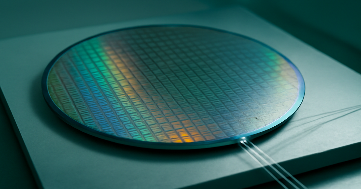
Researchers at the U.S. National Institute of Standards and Technology reported in Nature on April 15, 2026, that they have built photonic integrated circuits on silicon wafers capable of producing light at whatever wavelength is required, a step the agency said is aimed at shrinking the bulky, power-hungry laser systems that optical atomic clocks and quantum computers depend on.
The chips are made by coating a silicon wafer with silicon dioxide, or glass, and the non-linear material lithium niobate, according to NIST. Adding metal allows the conversion of light’s colour to be controlled electrically, and the metal–lithium niobate interface is used to switch light on and off at high speed. A second non-linear material, tantalum pentoxide or tantala, lets a single input colour be converted across the entire visible spectrum and a broad infrared band. NIST said the team spent years developing a way to fabricate tantala circuits without heating, so the material can be deposited on top of others without damaging them, and stacked the materials in three dimensions to transfer light efficiently between layers. A single wafer yields about 50 fingernail-sized chips carrying some 10,000 optical circuits, and the demonstrations covered wavelengths including the 980 nanometres typical of semiconductor lasers, the 780-nanometre red light used with rubidium and the 461-nanometre blue light used with strontium.
NIST said low-cost, low-power portable optical atomic clocks could support volcanic eruption and earthquake forecasting, navigation as an alternative to GPS, and dark matter research, with further possible uses in moving signals efficiently between AI chips and improving virtual reality displays. The chips are not yet in mass production; the work was carried out with Octave Photonics, a startup in Louisville, Colorado, founded by former NIST researchers, which is pursuing scale-up. The study (DOI 10.1038/s41586-026-10379-w) lists Grant M. Brodnik, Grisha Spektor and Lindell M. Williams as authors, along with Jennifer A. Black, Atasi Dan, Alexa R. Carollo and Jizhao Zang, plus David R. Carlson and Scott B. Papp.
A separate NIST team led by physicist Nikolai Klimov addressed a different obstacle to fielding such devices: how to attach optical fibers to photonic chips so the joint survives harsh conditions. In work published online on March 27, 2026, in Photonics Research and reported by NIST on March 30 (DOI 10.1364/PRJ.565679), the group adapted hydroxide catalysis bonding, a technique NASA has used to assemble ultra-precise optical systems, using a small amount of sodium hydroxide solution to fuse the surfaces of fiber and chip at the molecular level into an inorganic, glass-like bond.
Conventional organic polymer adhesives crack, outgas and degrade under cryogenic temperatures, radiation, vacuum and high heat, NIST said, and this is the first time hydroxide catalysis bonding has achieved both the alignment precision required for optical fibers and efficient optical coupling. The packaged chips were cryogenically cooled, subjected to rapid temperature swings, exposed to intense ionizing radiation and placed under high vacuum, and the bonds held while the chips continued to work. High-temperature testing of the packaged chips was not possible because of the limits of the commercial fiber used, although separate work confirmed the bond’s mechanical stability at temperatures far above those tolerated by existing adhesives.
NIST said photonic integrated circuits can move data at high speed using far less power than conventional chips, and listed space missions, reactor cores, particle accelerators, quantum computing platforms requiring ultra-high vacuum and cryogenic temperatures, and industrial and energy sensors as targets for the packaging. The bonding process currently takes several days, which the researchers described as an engineering challenge rather than a fundamental barrier, saying concentrated development could make it suitable for volume production. The paper credits Sarah H. Robinson, CH.S.S. Pavan Kumar and Ashutosh S. Rao; also named are Nikolai N. Klimov, Daron A. Westly, Glenn E. Holland, Thinh Q. Bui, Kevin O. Douglass, Fred B. Bateman and Daniel S. Barker. NIST noted that its article on the work was initially posted with an AI-generated image, which was removed.